Integrated Circuit Packaging:
As the mobile device sector demands smaller, cheaper and more functional IC packages, a technology gap has emerged in the IC substrate for feature dimensions 1-10um whereby conventional IC manufacturing methods are too expensive, and conventional PWB manufacturing methods cannot achieve the resolution required. “Laser Embedded Conductor Technology” enables conductors to be formed within the surface of the dielectric material, and thereby overcoming some of the manufacturing challenges associated with the technology gap.
Benefits of Laser Embedded Conductor Technology:
- Higher resolution than LDI, enabling the total layer count to be reduced, thereby reducing the size and cost of the package.
- Wiring and vias made in a single process.
- Near padless vias allow more routing space, further reducing the total layer count.
- The reduction in the conductor path length improves signal integrity.
- Embedding conductors improves surface planarity within a multi-layer substrate, reducing warpage issues.
- No requirement for photo-chemistry or blind-via drilling equipment.
- Superior Cu adhesion due to “3-point anchoring”.
- Standard low K, low CTE organic dielectrics may be used
Scanned Mask Imaging (SMI):
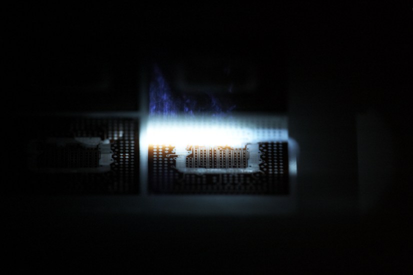
M-Solv’s proprietary technology “Scanned Mask Imaging” (SMI) allows direct patterning and ablative removal of materials down to a resolution of a few microns. A photo-mask is raster scan illuminated by a UV multi-mode solid state laser. A high resolution projection lens delivers a de-magnified image of the photo-mask to the substrate, where the energy is used to modify the target material.
This novel technology takes advantage of the low running costs associated with solid state laser systems, as well as the flexibility and quality of process offered by imaging systems. In comparison to excimer laser systems of equivalent specification, the process cost of ownership can be <50% using SMI technology, with no reduction in quality, and with higher throughput.
Contact us to find out more.
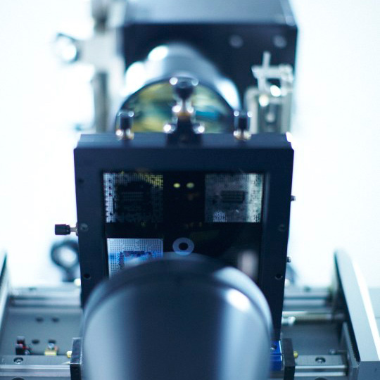
MSV 300
The MSV-300 is a high volume manufacturing machine designed for high resolution Laser Direct Ablation of organic substrates. The ablated structures enable embedded circuitry required for next generation IC substrates and interposers. Click here to view.
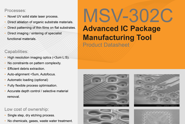
MSV 302C Product Datasheet
Looking in detail at the MSV-302C advanced IC package manufacturing tool, with information on its processes, capabilities, features and detailed specification. Click here to view.